← Gibson ES-335 Wiring Diagram: Vintage Tone Secrets! Gibson es 335 wiring diagram humbuckers iPhone 8 Inside Diagram – See What Makes It Tick! Exploring the inner workings of the iphone 8 plus: a diagram breakdown →
If you are searching about Pcb Design Differential Impedance Of Lvds Rules And T - vrogue.co you've came to the right web. We have 25 Images about Pcb Design Differential Impedance Of Lvds Rules And T - vrogue.co like Some LVDS PCB Layout Guidelines For Ensuring Signal, 40% OFF, Some LVDS PCB Layout Guidelines For Ensuring Signal, 40% OFF and also PCB Design Tutorial: Basic Rules, Tips and Guidelines-TechSparks. Here it is:
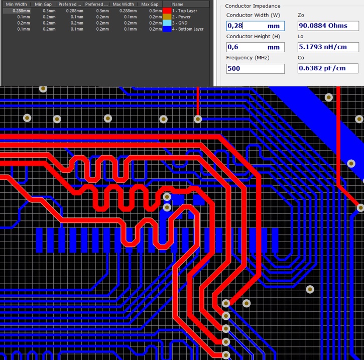
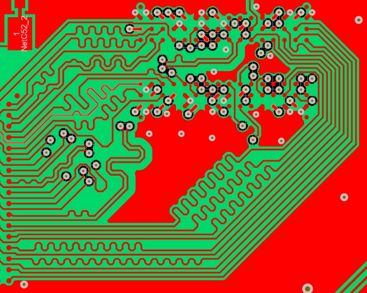
Pcb Design Differential Impedance Of Lvds Rules And T - Vrogue.co
 www.vrogue.co
Pcb Design Differential Impedance Of Lvds Rules And T - vrogue.co
Some LVDS PCB Layout Guidelines For Ensuring Signal, 40% OFF
 www.oceanproperty.co.th
Some LVDS PCB Layout Guidelines For Ensuring Signal, 40% OFF
PCB Design Tutorial: Basic Rules, Tips And Guidelines-TechSparks
 www.tech-sparks.com
PCB Design Tutorial: Basic Rules, Tips and Guidelines-TechSparks
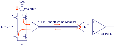
Some LVDS PCB Layout Guidelines For Ensuring Signal Integrity | PCB
 resources.altium.com
Some LVDS PCB Layout Guidelines for Ensuring Signal Integrity | PCB ...
Top 5 Pcb Design Guidelines In Electronics Industry 2 - Vrogue.co
 www.vrogue.co
Top 5 Pcb Design Guidelines In Electronics Industry 2 - vrogue.co
PCB Layout Guidelines And Considerations
 www.microcontrollertips.com
PCB layout guidelines and considerations
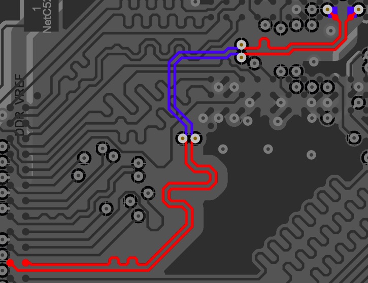
LVDS PCB Layout – Expert Guidelines You Need To Know! Pcb Layout Design
 superspotsz.blogspot.com
LVDS PCB Layout – Expert Guidelines You Need to Know! Pcb layout design ...
Some LVDS PCB Layout Guidelines For Ensuring Signal, 40% OFF
 www.oceanproperty.co.th
Some LVDS PCB Layout Guidelines For Ensuring Signal, 40% OFF
PCB Layout Design - ESP32-S2 - — ESP Hardware Design Guidelines Latest
 docs.espressif.com
PCB Layout Design - ESP32-S2 - — ESP Hardware Design Guidelines latest ...
PCB Schematic And Layout: A Comprehensive Guide – Hillman Curtis
 hillmancurtis.com
PCB Schematic and Layout: A Comprehensive Guide – Hillman Curtis ...
PCB Design Tips | Circuit Board Layout & Design Guidelines
 www.wellpcb.com
PCB Design Tips | Circuit Board Layout & Design Guidelines
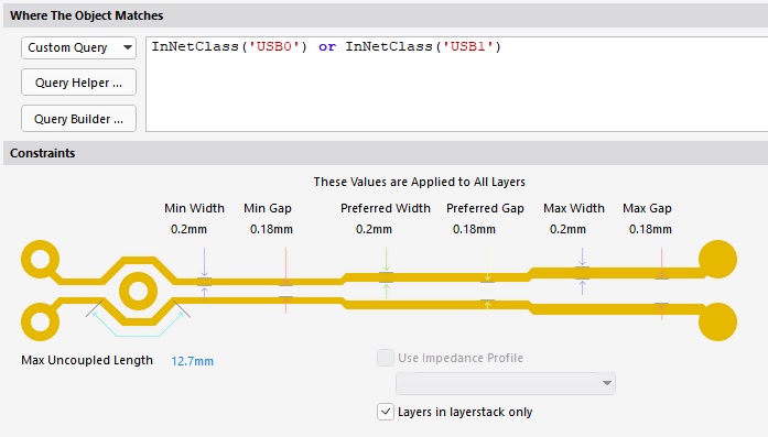
PCB Layout Guidelines For USB Type-C
PCB Layout Guidelines for USB Type-C
Comparison Of Routing And Layout Guidelines For UART, SPI, And I2C
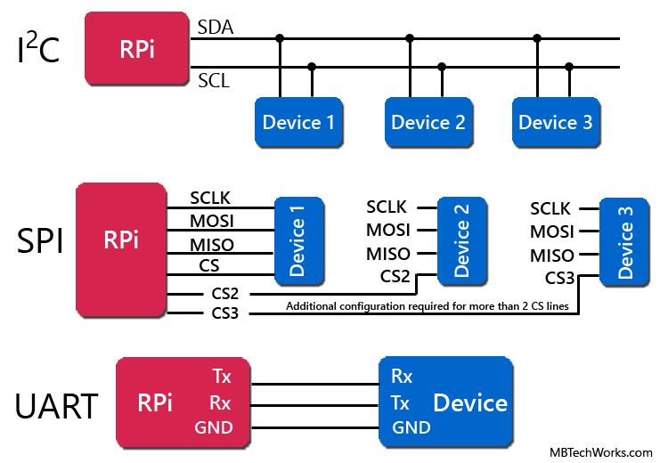 www.pcb-hero.com
Comparison of Routing and Layout Guidelines for UART, SPI, and I2C ...
Understanding LVDS Interface: A Comprehensive Guide
 www.shiningltd.com
Understanding LVDS Interface: A Comprehensive Guide
Main Design Guidelines & Layout Rules On High Speed PCB
 www.integrasources.com
Main Design Guidelines & Layout Rules on High Speed PCB
Main Design Guidelines & Layout Rules On High Speed PCB
 www.integrasources.com
Main Design Guidelines & Layout Rules on High Speed PCB
Some LVDS PCB Layout Guidelines For Ensuring Signal Integrity | PCB
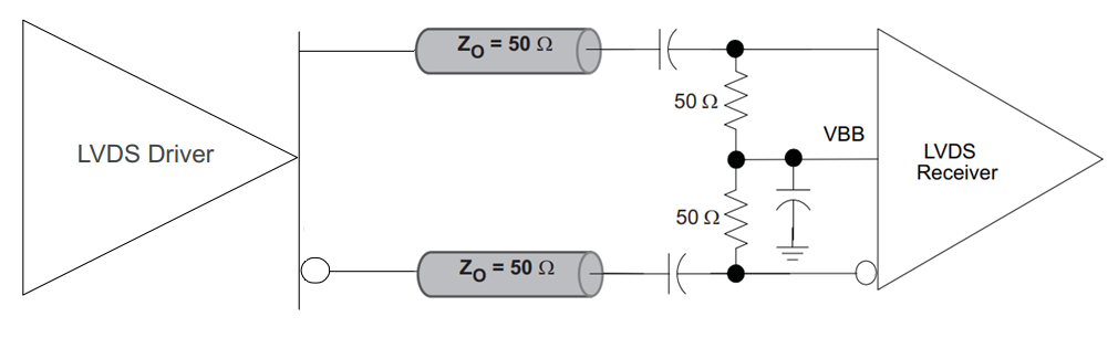 resources.altium.com
Some LVDS PCB Layout Guidelines for Ensuring Signal Integrity | PCB ...
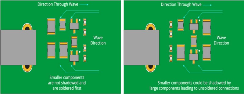
Component Placement In PCB Design & Assembly | Sierra Circuits
 www.protoexpress.com
Component Placement in PCB Design & Assembly | Sierra Circuits
PCB Design Guidelines For Reduced EMI (Electromagnetic Interference)
 oxeltech.de
PCB Design Guidelines for Reduced EMI (Electromagnetic Interference)
Main Design Guidelines & Layout Rules On High Speed PCB
 www.integrasources.com
Main Design Guidelines & Layout Rules on High Speed PCB
Main Design Guidelines & Layout Rules On High Speed PCB
 www.integrasources.com
Main Design Guidelines & Layout Rules on High Speed PCB
24. Top 5 PCB Design Guidelines Every PCB Designer Needs To Know,PCB Design
 www.juvtmall.com
24. Top 5 PCB Design Guidelines Every PCB Designer Needs to Know,PCB Design
Main Design Guidelines & Layout Rules On High Speed PCB
 www.integrasources.com
Main Design Guidelines & Layout Rules on High Speed PCB
Using SDRAM Vs. DDR RAM In Your PCB Design | Blog | Altium Designer
 resources.altium.com
Using SDRAM vs. DDR RAM in Your PCB Design | Blog | Altium Designer
Main Design Guidelines & Layout Rules On High Speed PCB
 www.integrasources.com
Main Design Guidelines & Layout Rules on High Speed PCB
Main design guidelines & layout rules on high speed pcb. Main design guidelines & layout rules on high speed pcb. Main design guidelines & layout rules on high speed pcb